


A small step for graphene, a giant leap for electronics and spintronics
13.11.2025
 |
|
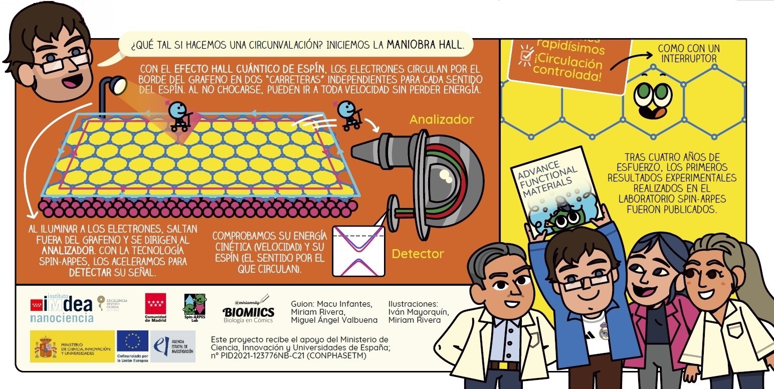
Excerpt from the comic "One small step for graphene, one giant leap for electronics and spintronics". Image: Miriam Rivera for IMDEA Nanociencia. |
- Researchers at IMDEA Nanociencia have succeeded in opening a bandgap in graphene by doping it with tellurium atoms.
- The study not only allows the flow of electricity in graphene to be controlled, but also enhances its properties related to electron spin.
| Tweet |
Madrid, 13th November 2025. Researchers at IMDEA Nanociencia have made a significant breakthrough in the engineering of graphene, a material renowned for its low resistance and very high conductivity, but whose lack of a natural ‘switch’ has hindered its use in electronic devices such as transistors. In this new study, scientists have found a way to overcome this limitation by opening a bandgap, or energy gap, that allows the flow of electricity in graphene to be controlled, an essential step for advanced technological applications.
The achievement is based on the controlled intercalation of tellurium (Te) atoms between layers of graphene deposited on an iridium base. Using spectroscopy, microscopy and electron diffraction techniques, the researchers observed that tellurium arranges itself into two different structures, depending on the amount used. Beyond this structure, what is truly revolutionary is that the modified graphene exhibits an energy gap of up to 240 millielectron volts at room temperature, something never before observed in a stable and adjustable form.
This new configuration not only allows the flow of electricity in graphene to be controlled, but also enhances its quantum properties related to electron spin. The study shows that electrons behave as if they all had the same type of spin according to their direction of propagation, a behaviour known as the quantum spin Hall effect. This is key to future spintronics, a technology that makes use of the spin property of electrons to achieve faster and more efficient devices than those manufactured with conventional electronics.
With this breakthrough, the team demonstrates that it is possible to design hybrid materials from graphene that combine electronic control and advanced quantum properties. If this structure can be replicated on insulating materials, this discovery could pave the way for a new generation of more efficient, faster and more compact electronic and quantum devices.
This breakthrough has been published in the journal Advanced Functional Materials and featured on its cover. Is the result of a collaboration between researchers at the Madrid Institute for Advanced Studies in Nanoscience, the Autonomous University of Madrid and the University of Calabria (Italy). It has been partially funded by the Severo Ochoa Excellence accreditation, awarded to IMDEA Nanociencia (CEX2020-001039-S) and by the Spanish Ministry of Science and Innovation through Grant. no. PID2021-123776NB-C21 (CONPHASETM).
Glossary
- Spin: magnetic angular momentum of electrons. Unlike the classical intuition of a particle spinning on its own axis, spin does not imply that the electron is actually rotating. Spin is a fundamental property that describes a type of angular momentum associated exclusively with subatomic particles, with no direct equivalent in classical physics.
- Spintronics: also known as spin electronics, this is a branch of physics that exploits not only the charge but also the spin state of electrons to devise data storage or transfer devices that are more efficient than current electronic devices.
- Bandgap: also called the forbidden band, determines the amount of energy needed for electrical conduction. When an electron possesses the bandgap energy, it is excited to a free state and can participate in electrical conduction.
Reference
B. M. Cano, F. Calleja, D. Pacilè, M. G. Cuxart, M. Pisarra, A. Sindona, F. Martín, E. Salagre, P. Segovia, E. G. Michel, A. L. Vázquez de Parga, R. Miranda, J. Camarero, M. Garnica, M. A. Valbuena, Engineering a spin-orbit bandgap in graphene-tellurium heterostructures. Adv. Funct. Mater. 2025, 2425154. DOI: https://doi.org/10.1002/adfm.202425154
![]() Link to IMDEA Nanociencia Repository: https://hdl.handle.net/20.500.12614/3982
Link to IMDEA Nanociencia Repository: https://hdl.handle.net/20.500.12614/3982
Contact:
Dr. Miguel Ángel Valbuena
Spin-Resolved ARPES group
https://nanociencia.imdea.org/es/spin-arpes/home
Dr. Manuela Garnica
Topological Surfaces States in Quantum Materials group
https://nanociencia.imdea.org/nanoscale-imaging-of-2d-materials/group-home
IMDEA Nanociencia Dissemination and Communication Office
divulgacion.nanociencia [at]imdea.org![]()
![]()
![]()
![]()
![]()
Source: IMDEA Nanociencia.
IMDEA Nanociencia Institute is a young interdisciplinary research Centre in Madrid (Spain) dedicated to the exploration of nanoscience and the development of applications of nanotechnology in connection with innovative industries.